EN

Perfectus-A Series

Atmospheric Pressure Silicon Epitaxy

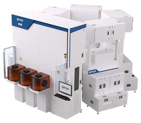
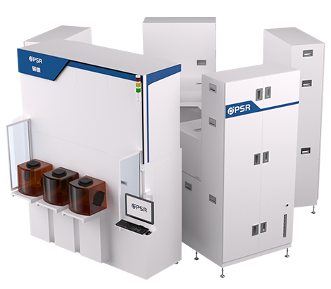
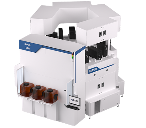
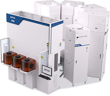
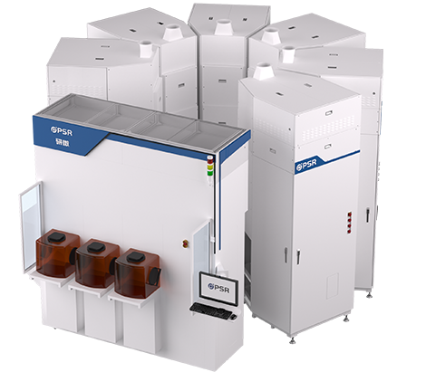
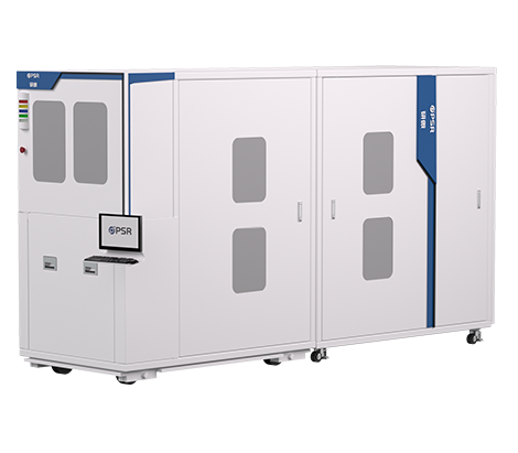
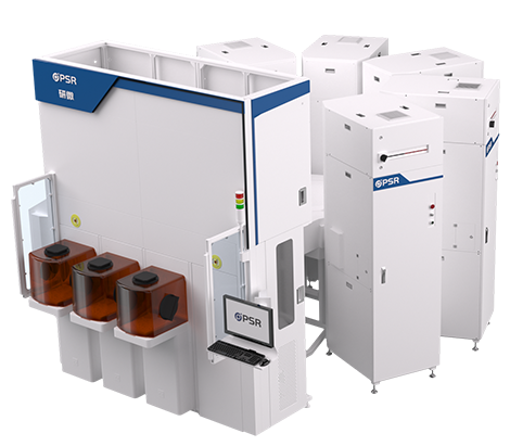
The silicon epitaxy process refers to the growth of a layer of single crystal material with the same lattice arrangement as the substrate on a single crystal substrate,Perfectus-A is mainly used for the growth of homogeneous epitaxial layers (Si/Si), used in the manufacturing of semiconductor discrete devices and integrated circuits.Epitaxy growth can improve the integrity of the CMOS gate oxide layer,channel leakage,and the reliability of integrated circuits by growing high-quality epitaxial layers

Market application

  • Silicon wafer epitaxial layer
  • Power devices
  • CIS Sensor
  • MEMS

Core advantages

Optimized reaction chamber design aided by CFD simulation to achieve performance requirements such as Wiw film thickness,doping uniformity and center-edge tunability;

Domestic software architecture achieves top machine stability,reliability and security,and multi-level hardware and software safety interlock testing;

Excellent software operating system and intelligent data analysis platform,the world's top technology/hardware customer support team.